Laboratory of micro- and nanosystem technology
Head of laboratory - Amirov I.I.Research areas
Research and development of plasma processes for micro- and nanosystem technology
The study of plasma-chemical etching processes of SiO2, Si, photoresist and polymer films in C4F8, CHF3, C4F8+Ar, SF6, O2 etc. and their mixtures
The study of plasma etching/deposition processes is carried out in a dense plasma reactor. It consists of the discharge and reaction chambers. The plasma is created in a quartz cylindrical chamber with two-coil inductor and RF generator (f = 13.56 MHz, W = 1.0 kW) in an inhomogeneous magnetic field of collateral type. From the discharge chamber plasma is distributed in the reaction chamber, in which the processed substrate is set on the cooled RF electrode. Application of a magnetic field allows increasing the density of the ion flux bombarding the surface of the substrate at several times and improving the uniformity of density distribution. The electron temperature near the substrate is 3-6 eV, Ne ~ 1011 cm-3. The ion energy is determined by the constant negative self-offset potential that arises when applying a given RF power to the electrode.


There is a thin-walled metal screen inside the reaction chamber. It is heated by plasma to a certain temperature, determined by the conditions of thermal balance with external walls of the reactor. In chemically active fluorocarbon plasma the speed of birth and death of radicals on the reactor walls, and consequently, their concentration, can be varied by controlling the temperature of the reactor walls.
- Amirov I.I., Izyumov M.O., Morozov O.V. Etching of Silicon and Silicon Dioxide in Dense Low-Pressure Inductively Coupled Radiofrequency Discharge Fluorocarbon Plasmas. // High Energy Chemistry. 2003. Vol. 37. No. 5. P. 328.
- Amirov I.I., Alov N.V. Polymer Film Deposition in Inductively Coupled Radio-Frequency Discharge Plasma of Perfluorocyclobutane Mixed with Sulfur Hexafluoride. // High Energy Chemistry. 2006. Vol. 40. No. 4. P. 267.
The processes of anisotropic and selective etching of SiO2 and deep etching of quartz
For the purposes of microelectronics and microtechnology anisotropic and selective etching processes of SiO2 (<100 nm) and deep etching of quartz (200 um) are developed in the fabricated reactor with hot walls. Hot walls increase more than twice the SiO2/Si etching selectivity and prevent deposition of fluorocarbon film on them, which is especially important in the long process of etching of quartz.

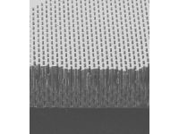
Nanowells in SiO2 layer (etching through the poly-Si (60 nm) mask in plasma CHF3 + Ar, the selectivity of the SiO2/Si > 10).
Processes of dimensional and anisotropic etching of silicon in fluorine-containing plasma SF6 + CHF3
For the purposes of microtechnology the processes of dimensional and anisotropic etching of Si were developed. By the dimensional etching of Si the ratio etching rate in vertical and horizontal directions can be controlled. With this etching method you can perform volumetric transfer of the mask pattern into the layer of silicon with different increases in height and width. This allows you to create, for example, a cone.

Through etching of quartz plates (200 um) through a Cr mask. Etching rate of 0.5 um/min, the selectivity with respect to Cr ~ 100.


Research and development of plasma processes of deep and anisotropic etching of silicon
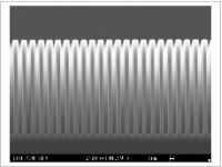
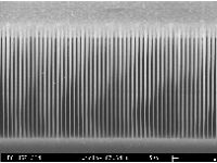
The research of processes of deep anisotropic etching of Si in a SF6/C4F8 plasma RFI-discharge (Bosch-process) for the forming of microstructures with high aspect ratio is performed. Etching rate of Si structures (A < 20) reached 4-6 um/min. The processes of through-wafer etching of Si are developed.
For the purposes of microtechnology in the fabricated reactor with the hot walls the processes of deep etching through the masks of photoresist, Si, SiO2, Cr in a circular, two-stage process of etching/passivation in SF6/C4F8 plasma (Bosch-process) are studied and developed. Anisotropic etching rate of Si was 10 um/min, the selectivity of etching of Si/SiO2 exceeded 200.
Study of the conditions for realization of aspect-independent etching in the Bosch-process was performed.

- Amirov I.I., Morozov O.V., Izumov M.O., Kaljnov V.A. and other. Plasmachemical Etching of High Aspect Ratio Deep Trenches in the Silicon for the Creation of the Various Elements of micromechanics. // Journal of Nano and Microsystem Technique. 2004. V. 12.
- Амиров И.И., Морозов О.В., Постников А.В., Кальнов В.А., Орликовский А.А., Валиев К.А. Плазменные процессы глубокого травления кремния в технологии микросистемной техники. Труды ФТИАН. Квантовые компьютеры, микро-наноэлектроника. М.Наука. 2009.Т.20. С.159-174.
Simulation of forming of Si microstructures with high aspect ratio in the Bosch-process
Method for two-dimensional simulation of the cyclic etching/passivation process (Bosch - process) of the formation of deep grooves in Si is developed. The method is based on the method of cells for the evolution of the surface profile of the structures and the Monte Carlo method for generation of plasma flows.
The simulation method is implemented in an interactive software system that provides ample opportunities for the numerical simulation experiments.
With the help of the developed method the simulation of the forming of deep high-aspect (A > 10) grooves with submicron dimensions in Si by the Bosch-process in SF6/C4F8 plasma was carried out. Comparison of simulation results with experimental data confirms the validity of the model. It is shown that in aspect-independent etching of deep grooves in Si the rate of process is determined by the rate of delivery of the fluorine atoms on the bottom of the deep grooves.
Simulation confirms the existence of a wide range of distortion effects of the grooves profile by etching Si in the Bosch-process in SF6/C4F8 plasma. It is shown that it is possible to vary the shape of sub-micron grooves by changing the control parameters during the process. Conditions for the formation of grooves with different angles of inclination of side walls, the origin of the aperture effect and the achievement of aspect-independent etching were determined.


- Shumilov A.S., Amirov I.I. Modeling of Deep Grooving of Silicon in the Process of Plasmochemical Cyclic Etching/Passivation. // Russian Microelectronics. 2007. Vol. 36. No. 4. P. 241.
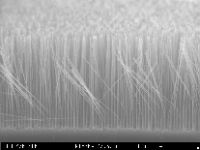
- Amirov I.I., Alov N.V. Formation of Microstructures on Silicon Surface in a Fluorinated Plasma via the Cyclic Etching–Passivation Process. // High Energy Chemistry. 2008. Vol. 42. No. 2. P. 132.
- Shumilov A.S., Amirov I.I. The Mechanism of Formation of Microneedles on the Silicon Surface in Fluorinated Plasma via the Cyclic Etching–Deposition Process. // High Energy Chemistry. 2008. Vol. 42. No. 5. P. 399.
Development and fabrication of micro- and nanoelectromechanical devices (micro- and nanoresonators, microactuators, microaccelerometers, switches etc.)
Techniques for fabrication of inertial sensors, actuators and resonators have been developed on the basis of plasma processes of deep anisotropic etching of silicon. It allows fabrication of three-dimensional structures. In the fabrication of microaccelerometer there were used plasma processes of bulk Si etching and etching of high aspect ratio microstructures.
For the manufacturing of microactuators with a large range of movement a new technology was developed. It is based on the concept of isolated SiO2 units formation in the bulk silicon wafer. It allows receiving electrically isolated trace elements on the plate without use of expensive SOI wafers. With this technology an electrostatic microactuator with a range of movement of 10 um and a driving voltage of 24 V has been manufactured.
Electro-static capacitive cantilever microswitches (three-layer cantilevers and bridges – Cr/Al/Cr with a thickness of 50/250/50 nm) were fabricated. Frequency response characteristics were measured. The main resonant frequencies of microcantilevers were located in the range of 10 kHz.


Nanocantilever resonators were fabricated. Cantilever had a thickness of less than 100 nm. There were also three-layer cantilevers (Cr/Al/Cr). Cantilevers had a length of 20 to 40 um and a width of 2 to 6 um. The measured resonant frequencies of cantilevers were up to 1 MHz.


- A. V. Postnikov; I. I. Amirov; V.V. Naumov; V. A. Kalnov. Simulation, fabrication, and dynamics characteristics of electrostatically actuated switches. // Proceedings of SPIE. 2008. Vol. 7025.
Measurement of dynamic characteristics of micro-and nanomechanical elements
Experimental setup for measurement of the dynamic characteristics of MEMS and NEMS sensitive elements (SE) was fabricated. Measurements were based on the method of the "optical lever": mechanical vibrations of SE were detected by the deflection of the laser beam reflected from its surface. Dynamic characteristics of SE (resonant frequencies, Q-factors) were determined from the resonant curve. Setup is assembled on an optical table.


Advantages of the experimental setup:
- - The size of the laser spot focused on the SE surface ~ 5 um;
- - Setup can record angular deviation of SE in the same plane (two-segment photodetector) and simultaneously in two planes (four-segment photodetector);
- - The range of measured resonance frequencies and quality factors of SE is limited only by capabilities of driving generator, photodetector and voltmeter. Replacement any of these devices does not require to reconstruct the optical system of the setup;
- - Vacuum system of the stand allows you to test SE at air pressures ranging from 10-4 to 105 Pa. This pressure range is wide enough to test SE in any of the available modes of air damping;
- - "Optical lever" does not require to connect a sample to a complex electronics (unlike, for example, the capacitive method of displacement detection). It is necessary just to focus the laser beam on the sample surface and excite oscillations of the sample in some way;
- - The stand is easily adjusted and modified (for example, a large vacuum chamber with a lot of vacuum inlets allows filling a chamber with various gases, heating or cooling of the sample).


- Уваров И.В., Козин И.А., Амиров И.И. Исследование влияния давления воздуха на динамику чувствительного элемента микромеханических устройств. // Вестник ЯрГУ. Серия Естественные и технические науки, 2010, №2, стр. 38-42.
- Uvarov I.V., Morozov O.V., Kozin I.A., Postnikov A.V. and other. Dynamic Characteristics of the Sensing Element of Microaccelerometer with Increased Damping Factor. // Journal of Nano and Microsystem Technique. 2011. V. 12.
- Kozin I.A., Postnikov A.V., Morozov O.V. Dynamics Study of Micromechanical Devices with Surface Metallization. // Journal of Nano and Microsystem Technique. 2011. V. 12.
- Uvarov I.V., Naumov V.V., Aminov M.K., Kupriyanov A.N., Amirov I.I. Analysis of Resonance Characteristics of Metal Micro-and Nanobeams. // Journal of Nano and Microsystem Technique. 2011. V. 12.
Research and development of the processes of magnetron deposition of metal, semiconductor and dielectric films for the purposes of microtechnology
Based on the study of the effect of ion bombardment on the properties of the deposited metal films following unique processes were developed:
- - Epitaxy of niobium on a sapphire substrate at room temperature. Without using it the substrate temperature must be at least 600 °C.
- - Deposition of highly textured metal films having electrical conductivity as the bulk metals. Usually, the conductivity of thin-film metal is worse than the bulk.
- - Deposition of CrOx durable coatings on the head reading information from magnetic tape (tape drives). Head life was increased by 3 times.
- - Development of antidiffusion coatings for gas turbine blades and aircraft engines. AlOx coating with varying oxygen content was located on the surface of the blade before deposition a protective layer of ZrO2, to prevent the diffusion of oxygen into the blade from this layer. The critical temperature at which diffusion starts was raised from 800 °C to 1000 °C.
The processes of deposition of ultrathin magnetic films for multilayer structures with giant magnetoresistance (GMR) were developed. Magnetic properties of such films and structures were investigated by magnetooptical method (equatorial Kerr effect).


Longitudinal (dashed lines) and transverse (thick lines) magnetoresistance of Co/Cu/Co structures received: a) using bias, b) without bias.
- Naumov V.V., Buchin E.Yu. Magnetoresistance of Multilayered Structures Obtained by the Magnetron Method. // Russian Microelectronics. 2009. Vol. 38. No. 5. P. 334.
- Naumov V.V., Bochkarev V.F, Buchin E.Yu. Increasing adhesion of metallic films to silicon by ion bombardment during growth. // Technical Physics. 2009. V. 54. N. 7. P. 1072.
- Naumov V.V., Paporkov V.A., Lokhankin M.V. Dependence of the Transversal Magneto-Optic Kerr Effect on the Incidence Angle of Light for Ultrathin Films of Cobalt and Co/Cu/Co Multilayers. // Russian Microelectronics. 2009. Vol. 38. No. 4. P. 251.